Custom FOC Driver PCB
Overview
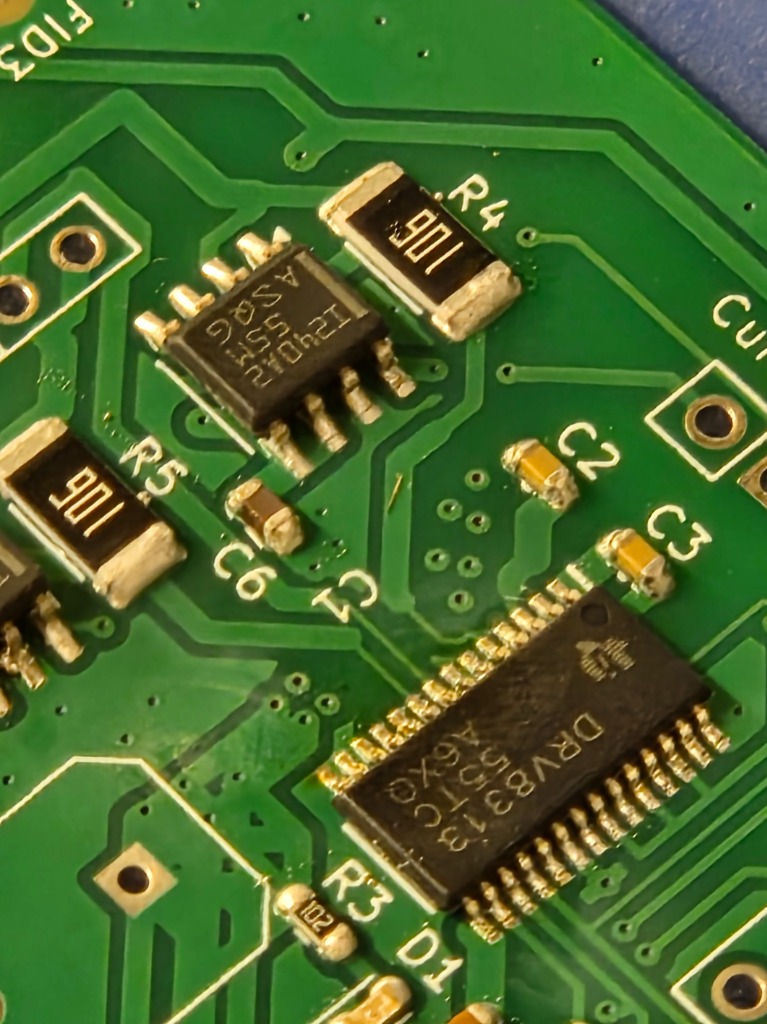
This project documents the design, assembly, and bring-up debugging of a custom BLDC motor driver PCB built around the Texas Instruments DRV8313 three-phase gate driver. The board includes inline phase current sensing using two Texas Instruments INA240A2D current sense amplifiers. What started as a straightforward motor spin-up turned into a rigorous multi-domain diagnostic exercise spanning firmware, power electronics, and IC datasheet analysis.
PCB Design
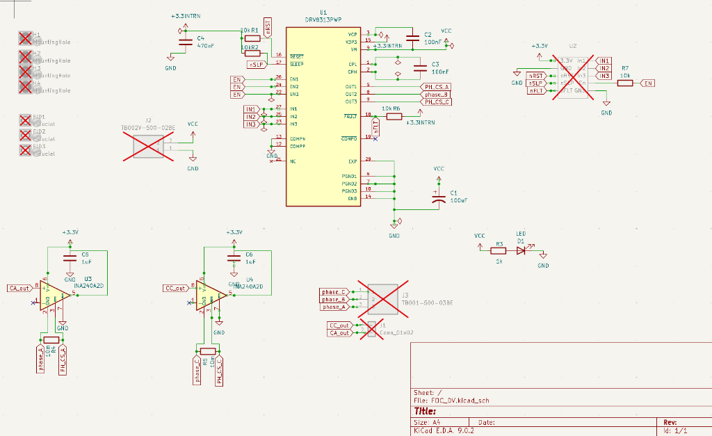
The driver is built around the DRV8313 gate driver IC in a 28-pin HTSSOP package, designed in KiCad. The board includes:
- Two INA240A2D inline current sense amplifiers on motor phases A and C, allowing the third phase current to be derived by Kirchhoff's current law
- A separate analog power rail (
+3.3VADC) to isolate the current sense amplifier supply from the noisy digital domain, reducing ADC noise floor - 100uF bulk decoupling on the motor supply rail and 100nF ceramic bypass caps on the gate driver logic supply
- Three-phase motor terminal block (TB001-500-03BE) with a 2x5 SWD header for STM32 programming
- Status LED with a 1k series resistor on the gate driver fault indicator
Initial Testing: Six-Step Commutation
The first bring-up attempt used a six-step (trapezoidal block) commutation script running on an STM32 microcontroller to command the DRV8313. The motor produced zero response: no movement, no current draw.
Before assuming a hardware issue, I needed to rule out the firmware layer entirely.
1. Firmware Layer Verification
The STM32 has a significantly more complex hardware timer matrix compared to standard AVR microcontrollers. My initial hypothesis was a software-level timer mapping failure inside the motor control library.
Action: Bypassed the motor control library entirely. Wrote a minimal C++ test using analogWrite() to generate a raw 490Hz, 50% duty cycle square wave directly across the three PWM output pins, with no library abstraction in the signal path.
Result: Oscilloscope verification confirmed three clean 5.0V square waves at the MCU output pins.
Conclusion: The MCU and firmware were generating valid PWM logic. The failure resided in the power stage or driver interface.
2. Driver Board Diagnostics (Power Stage Domain)
With firmware confirmed good, I focused on the driver board itself. The 6-step commutation script was still active, the motor still drew zero current, and the fault pin showed no error.
Action: Probed the DRV8313 output phases (OUT1/2/3) and the fault pin (nFAULT).
Result: nFAULT read logic HIGH, indicating the chip was not in an overcurrent or thermal shutdown state. However, the output phases showed flat 0V lines instead of the expected 12V amplified PWM.
Conclusion: The driver was structurally intact but actively refusing to switch its internal FETs.
3. Logic Level and Interface Analysis (Hardware Domain)
I moved the oscilloscope probe to the control inputs of the DRV8313 to verify signal integrity between the MCU and the driver.
Action: Probed the EN (Enable) pin, which must be driven HIGH to wake the chip from its low-power state.
Result: The oscilloscope recorded an anomalous 3.6V floating voltage on the EN pad, rather than the expected 5.0V logic HIGH from the STM32.
4. Datasheet Root-Cause Analysis
To understand the 3.6V anomaly, I consulted the Texas Instruments DRV8313 datasheet.
Electrical Characteristics: The datasheet specifies an internal 3.3V LDO regulator that powers the chip's core logic. Without a shared ground between the STM32 and the driver board, the EN pin had no valid return path for the logic signal. Instead of sitting at 0V (logic LOW) or 5V (logic HIGH), it floated to the chip's internal logic supply rail (~3.3V) plus a parasitic offset, settling at approximately 3.6V.
Truth Table Analysis: According to the IC's logic table (Table 1), if the ENx pins do not register a clean logic HIGH, the output H-bridges default to a High-Impedance (Hi-Z) state, essentially acting as an open circuit. This explained the flat 0V output phases despite the fault pin reading healthy.
Resolution
The floating intermediate voltage identified a missing common ground reference between the 5V MCU logic domain and the driver's isolated logic rail. By establishing a unified 0V reference and correctly leveling the enable pin to match the driver's internal thresholds, the DRV8313 successfully exited the Hi-Z state. The PWM signals amplified correctly and the motor spun.
Inline Current Sensing
With the driver functional, I turned to the board's primary differentiating feature: inline current sensing on motor phases A and C.
Why Inline Current Sensing
Standard voltage-mode FOC drives the motor by commanding voltage vectors and relies on estimated current. Measuring actual phase current closes a real torque feedback loop, enabling load rejection and precise torque control without tuning around model uncertainty.
Topology
The INA240A2D is a bidirectional, zero-drift current sense amplifier with 50V/V fixed gain and enhanced PWM rejection. The PWM rejection is critical: during motor commutation, the common-mode voltage across the shunt swings rapidly with the switching transients. The INA240 uses an internal filter that suppresses this switching noise, allowing accurate current readings even in the middle of a PWM cycle.
Two INA240A2D amplifiers are placed inline on phases A and C. Because the three phase currents in a star-connected motor must sum to zero (Kirchhoff's current law), sensing two phases lets the firmware derive the third mathematically without a third amplifier.
Signal Chain
The voltage drop across each shunt resistor is amplified 50x by the INA240 and fed to the STM32 ADC. The amplifier supply uses a dedicated +3.3VADC rail on the PCB, separated from the noisy digital +3.3V rail. This analog-digital power domain separation reduces switching noise coupling into the ADC reference, which would otherwise appear as a DC offset or noise floor in the current measurement.
The SimpleFOC InlineCurrentSense class is configured with the measured shunt resistance and 50 V/V gain, mapping ADC counts back to amps in firmware.
Validation
After the ground fix, I confirmed current sense operation with an oscilloscope across each shunt. The amplified output at the INA240 output pin tracked the expected sinusoidal phase current envelope during six-step commutation, with no visible saturation or common-mode noise artifacts. The readings matched the expected peak current calculated from the DRV8313 supply voltage and motor winding resistance.
Skills Demonstrated
| Area | What Was Done |
|---|---|
| PCB Design | KiCad schematic and layout, analog/digital power domain separation, SMD component selection |
| System-Level Debugging | Methodical isolation of faults across software abstraction layers, MCU hardware timers, and power electronics |
| Test and Measurement | Proficient use of oscilloscopes for validating digital logic integrity, power stage outputs, and current waveforms |
| Datasheet Navigation | Cross-referencing anomalous hardware behaviors with manufacturer electrical specifications and truth tables to determine IC states |
| Firmware Engineering | Writing minimal C++ hardware tests to bypass complex libraries during root-cause analysis |
| Analog Design | Inline current sensing topology using INA240A2D, shunt sizing, ADC reference isolation |